

Wafer Fab Equipment: inside the machine shop behind AI


Updated 10 Nov 2026•6 min read

Over the past few editions we have looked inside the AI data center: the chips, the memory, the networking, the power. Today we go one step back, to the factories where those chips are made and the machines that fill them.
It starts with an empty building
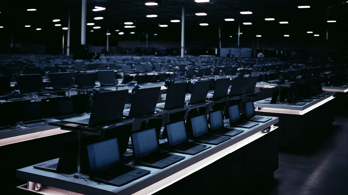
A leading-edge chip factory, or fab, costs upwards of $20bn and takes two to three years to build. Most of that money does not go into the building at all. It goes into the machines inside, called wafer fab equipment. At the heart of the fab is the cleanroom, a hall several football fields long where the air is constantly filtered. A single speck of dust is large enough to ruin a chip. Workers wear full-body suits, and most of the work is done by robots that carry sealed pods of wafers along tracks in the ceiling.
A wafer goes in
Every chip begins as a polished disc of pure silicon about the size of a dinner plate, called a wafer. Over roughly three months it moves from machine to machine through more than a thousand steps. The same five-step loop repeats hundreds of times, building the chip up one microscopic layer at a time:
- Deposition coats the wafer with a film of material, sometimes just a few atoms thick. Applied Materials leads here, alongside Lam Research, Tokyo Electron and ASM.
- Lithography prints the circuit pattern onto that film using light, much like a photographic negative. ASML makes the most advanced of these machines, and Tokyo Electron makes the systems that coat and develop the wafer around them.
- Etching carves away everything outside the pattern. Lam Research is the leader here.
- Polishing and treatment flatten the surface and adjust the material’s properties, so the next layer can go on cleanly. This is largely Applied Materials’ territory.
- Inspection checks every layer for defects before the next one goes on. KLA dominates here.
Lithography takes the largest share of spending at about 29%, followed by deposition at 23% and etch at 19%. The remaining 29% is split roughly evenly between polishing and treatment, and inspection.
Then the chips are put together
When the last layer is done, the wafer is cut into individual chips. For the chip in a phone or laptop, that is close to the end of the line. It is mounted on a small board and connected to the rest of the device. An AI processor is different. It is assembled from several chips, with a large processor in the middle surrounded by stacks of high-bandwidth memory placed just millimetres away, so data can reach the processor fast enough. Each stack is a dozen or more memory chips piled on top of one another, and the connections between them are so fine that making them takes the same deposition, etch, polishing and inspection machines used in the fab. This final stage, known as advanced packaging, has become one of the fastest-growing sources of demand for equipment makers.
Every new generation is hungrier than the last
Each generation of chip has more layers to build and less room for error, so it needs more machines. A wafer at the newest 1.4-nanometre generation takes about 60% more equipment spending than one at 5 nanometres. So a fab making the same number of wafers as one built only a few years ago needs far more equipment inside it.
Too much demand, too few fabs
AI has created capacity constraints at chipmakers’ fabs. Their best factories are running flat out, and their biggest customers are signing contracts years in advance, so they know demand will outrun supply until at least 2028. The only fix is to build, and everyone is building at once. TSMC has nearly 20 fabs in the works across Taiwan, the US, Japan and Germany, and says its 2-nanometre capacity will more than double next year. SK hynix and Samsung are racing to finish new memory fabs in Korea, pulling construction forward by months. Japan is backing Rapidus, a start-up building a 2-nanometre fab in Hokkaido that will ramp to around 25,000 wafers a month.
Then there is Terafab
Elon Musk’s Tesla and SpaceX have reportedly told equipment suppliers of their bold plan to target about 1 million wafers a month by 2032 at a single complex in Texas, with 70% for memory and 30% for logic. The memory side alone would match Samsung’s entire DRAM capacity today, and the logic side would be roughly equal to TSMC’s 2- and 3-nanometre capacity combined. The project starts with $55bn and could grow to $119bn, and at more than 100 million square feet it would have about 15 times the floor area of the Pentagon. A prototype fab is due to be finished in July 2027, Intel is lined up to provide its 2- and 1.4-nanometre technology for the logic side, and orders have already gone out to Japanese equipment makers. No chipmaker has ever gone from nothing to that size in six years, but for toolmakers, the orders are already real.
The result is a spending boom
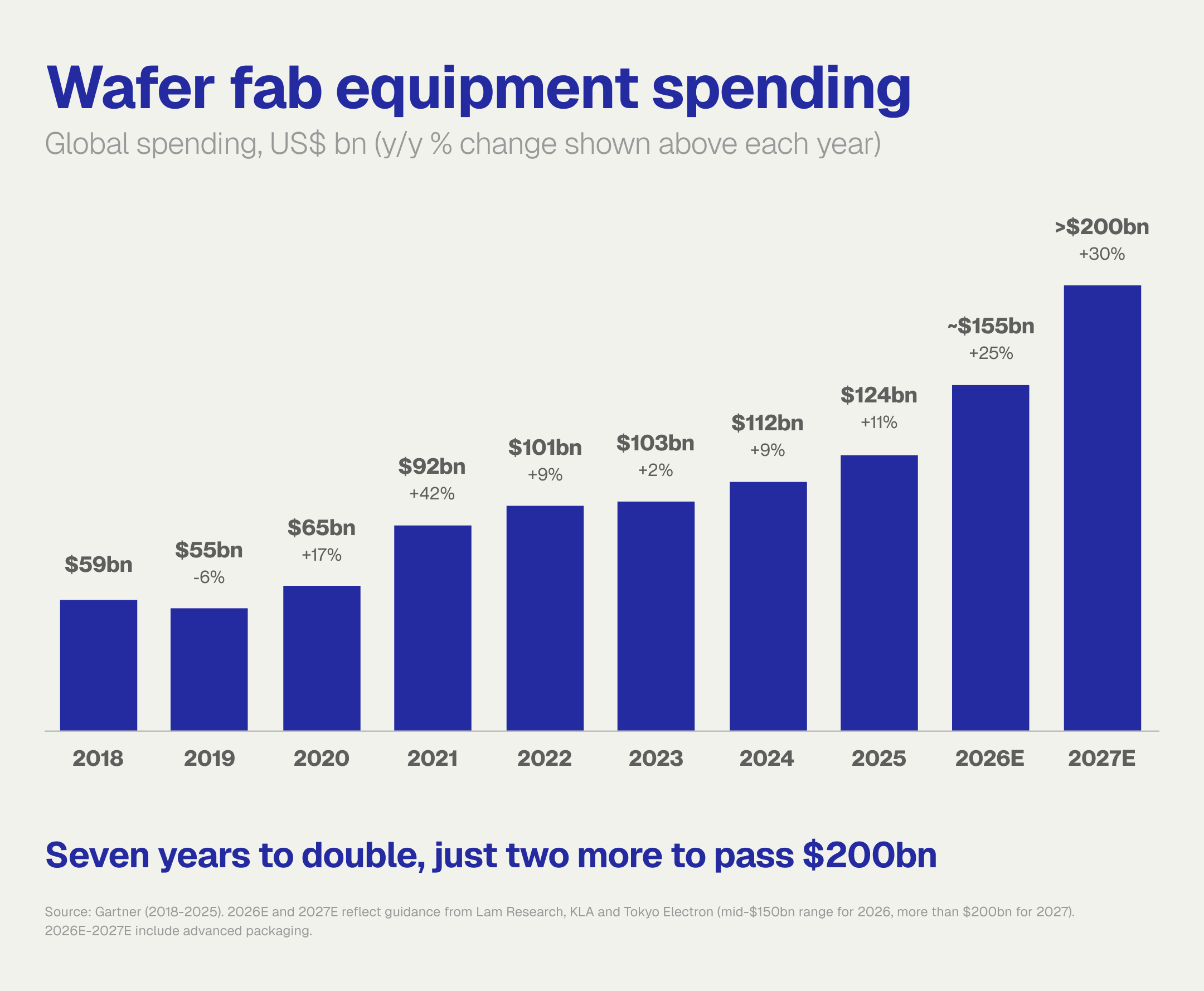
More fabs, each needing more machines, is why spending on chipmaking equipment is jumping. It took seven years for spending to roughly double, from $59bn in 2018 to $124bn in 2025. This time it is set to pass $200bn in 2027, adding more in two years than in the previous seven. As recently as March, KLA expected that level only by 2030. Roughly 60 cents of every dollar chipmakers spend on capex goes on these machines, and Applied Materials expects about 80% of the growth to come from the three areas AI leans on most, namely the most advanced logic chips, DRAM memory and advanced packaging.
What the toolmakers are saying
Every major supplier has raised its outlook this year. ASML expects sales to rise about 36% to €44–45bn, with system sales to memory makers up around 75%. It is already taking orders for 2028, and even with 30% more capacity next year it does not expect to meet demand. Applied Materials says its largest customers now share rolling two-year forecasts, with some conversations reaching 2030, and it is hiring to double its quarterly output by 2028. Lam expects its equipment sales to grow well over 40% this year, but warns that cleanroom space and component shortages are capping what the industry can ship. Space is so tight that Applied now markets one memory tool on the fact that it takes up 20% less floor space. KLA calls its sales visibility unprecedented, and both KLA and Applied expect their packaging revenue to grow more than 70% this year. ASM expects industry growth of more than 30% next year. Tokyo Electron puts it most simply. “More tokens, more semiconductors.”