How is India strengthening its position in Global Semiconductor Ecosystem
India is actively positioning itself as a major player in the global semiconductor ecosystem, transitioning from an importer to a significant manufacturing and design hub.
Key Takeaways
- India's semiconductor market, valued at $34 billion in 2023, is projected to surge to $215 billion by 2033, fueled by strong domestic demand and global supply chain diversification.
- Government initiatives like the India Semiconductor Mission and Production-Linked Incentive (PLI) schemes are attracting substantial investments, including over ₹1.6 lakh crore in announced projects from global and Indian firms.
- This strategic shift, leveraging India's design talent and cost advantages, signifies a powerful new growth engine for the economy, creating long-term opportunities across the technology value chain.
Ever wondered what really powers your phone, your car, or even that smartwatch tracking your steps?
Chips, tiny pieces of silicon that quietly run our lives. From AI models learning to think like humans to electric cars sensing every turn, these chips have become the new oil of our world.
Every country wants a piece of this power. And India is no different. With a $10 billion push, it’s gearing up to move from being a chip importer to becoming a serious chip maker
We’ve done it before, remember when India imported every mobile phone it used?
Today, we’re exporting them. And by 2027, half of Apple’s iPhones could be made here.
Now, the big question is, can we do the same with semiconductors?
Let’s find out…
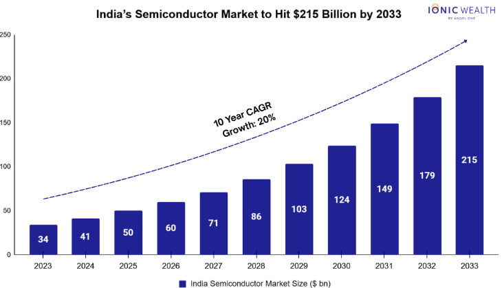
1. India is set to be one of the fastest-growing semiconductor markets..albeit on a smaller starting base.
For years, India watched the chip race from the sidelines. While the world built fabs and processors, we focused on the software that powered them. But the story is shifting.
From smartphones to electric vehicles, India’s hunger for semiconductors is growing rapidly. The market, valued at $34 billion in 2023 and mostly import-dependent, is expected to reach $215 billion by 2033, making it clear that building chips in India is no longer optional, it’s an opportunity waiting to be seized.
Importantly, India already has a solid foundation to build on. With a strong base of MSMEs in equipment manufacturing, access to critical materials, and engineers, we are already designing chips for global leaders such as Intel and Qualcomm.
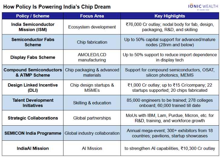
2. How policy is powering India’s chip dream
To turn this potential into reality, India needed direction. That’s where the government’s focused policy push comes in.
Over the past few years, India has introduced a series of initiatives to strengthen its semiconductor ecosystem. Programs like the India Semiconductor Mission, Production-Linked Incentive (PLI) scheme, and Design-Linked Incentive (DLI) are driving investments across chip fabrication, packaging, and design. Together, they aim to build a complete value chain and position India as a global hub for semiconductor manufacturing.
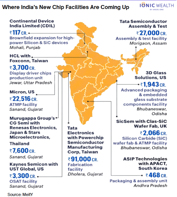
3. Major semiconductor projects announced in India
Policy is now turning into progress as we see the first wave of semiconductor projects already taking shape across the country, with both Indian conglomerates and global giants committing billions of dollars to set up local facilities.
From Tata Group’s fabrication partnership with Powerchip of Taiwan to Micron’s ATMP (Assembly, Testing, Marking, and Packaging) plant in Gujarat, these projects mark India’s transition from planning to production.
Together, these ventures represent over ₹1.6 lakh crore in investments and are laying the groundwork for India’s semiconductor manufacturing future.
4. What is powering India’s semiconductor momentum
India’s semiconductor rise is being shaped by two key forces, strong market growth and strategic structural enablers. On one hand, booming demand across electronics, EVs, and AI is driving the need for chips.
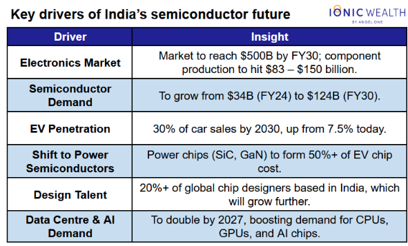
On the other hand, beyond policy support, factors like China+1, cost benefits and a strong engineering base are helping India emerge as a serious chip manufacturing hub:
a. Cost Advantage
India’s monthly manufacturing wage averages around $195, far lower than China’s $826, making it an attractive destination for global firms diversifying supply chains.
b. China + 1 and Geopolitical Realignment
India is becoming a key alternative to East Asia for assembly, testing, and packaging (Outsourced Semiconductor Assembly and Testing), areas where cost and scale matter most.
c. Design and Talent Strength
Over 120 global chip firms run design centers in Bengaluru, Hyderabad, and Noida. Government programs are also training 85,000+ engineers for manufacturing and design roles.
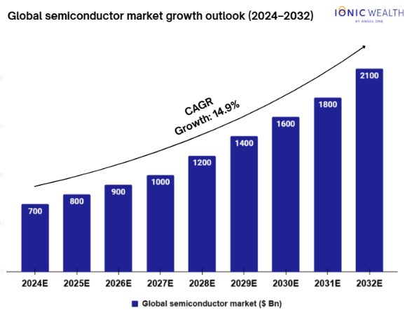
5.1 The global semiconductor market is mature and growing
While India builds its base, the rest of the world is racing to secure its chip future. According to Avendus Spark report, the global semiconductor market is projected to grow from $700 billion in 2024 to over $2100 billion by 2032.
The biggest growth drivers are demand for:
- CPUs, GPUs, and memory chips to power the next wave of AI.
- Chips for EVs and autonomous systems growing at 10%+ CAGR.
- High-performance chips in smartphones, appliances, and wearables.
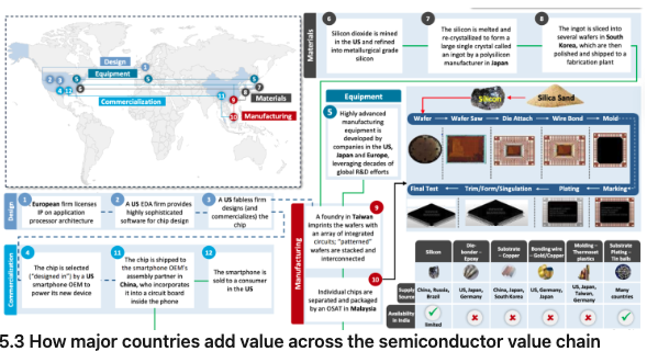
5.2 Global Semiconductor Chain: A Truly Borderless Industry
The semiconductor supply chain is vast, spanning over 70 countries, each playing a unique role in a highly interdependent ecosystem, which means No single country can make a chip alone. Here’s how this chain works:
Design Phase
IP Licensing: A European firm licenses the chip’s core architecture (for example, ARM).
EDA Software: A US-based Electronic Design Automation (EDA) company like Synopsys or Cadence provides advanced design tools.
Fabless Design: A US fabless semiconductor company (like Qualcomm or NVIDIA) uses these tools to design and commercialize the chip.
Chip Selection: A US smartphone maker (like Apple) chooses this chip to power its new device.
Materials & Manufacturing Phase
Equipment Development: High-end semiconductor manufacturing equipment is produced in the US, Japan, and Europe after decades of R&D.
Raw Material Extraction: Silicon dioxide is mined in the US and refined into metallurgical-grade silicon.
Crystal Formation: The silicon is melted and re-crystallized into large ingots by a polysilicon manufacturer in Japan.
Wafer Processing: These ingots are sliced into wafers in South Korea, polished, and sent to fabrication plants.
Fabrication: In Taiwan, foundries like TSMC imprint circuits onto the wafers, forming the chip’s layers.
Packaging & Testing: In Malaysia, the wafers are cut, tested, and packaged by OSATs (Outsourced Semiconductor Assembly and Testing firms).
Commercialization Phase
Assembly: The finished chip is shipped to a smartphone manufacturer’s facility in China, where it’s mounted on circuit boards.
Global Sale: The final product (a smartphone) is then sold to consumers worldwide, including in the US.
These phases show how creating a single chip is a truly global effort, a seamless collaboration of ideas, materials, and manufacturing spread across continents, powering the devices that run our world.
5.3 How major countries add value across the semiconductor value chain
The semiconductor industry operates through a globally specialized structure, with each region excelling in specific stages of production.
The US leads high-value segments like chip design (47%), EDA software (96%), and core IP (52%), reflecting its dominance in innovation and intellectual property.
Taiwan remains the global center for chip fabrication (19%), contributing significantly to advanced manufacturing and foundry services.
Japan adds strong value in wafers (56%) and fabrication tools (29%), while South Korea leads in fabrication (22%) and assembly (13%), driven by its focus on memory and materials.
Europe specializes in fabrication equipment (23%) and core IP (43%), strengthening its position in precision tools and semiconductor technology.
China’s value addition is concentrated in assembly, testing, and packaging (14%), though it is rapidly investing to expand into higher-value segments like design and fabrication.
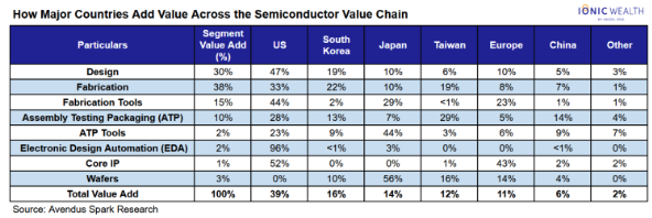
For India, this interconnected structure presents a chance to build deeper integration into the global ecosystem. With strengths in design, testing, and R&D, India can scale up capabilities in fabrication and materials through strategic policy initiatives and partnerships.
5.4 Who leads what in the global semiconductor chain?
To understand how global players fit together in this ecosystem, here’s a snapshot of the entire semiconductor value chain, from chip design to end-product manufacturing.
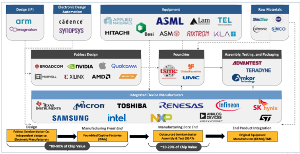
This shows how each stage is dominated by different players. It clearly reflects how the chip industry is both deeply specialized and globally interlinked, each company and country contributing a crucial piece of the puzzle.
6.1 Where India stands in the global semiconductor supply chain
India may be new to large-scale chip fabrication, but it already plays a pivotal role in design, testing, and system innovation. Global Capability Centers (GCCs) of firms like Intel, Qualcomm, and Texas Instruments have made Bengaluru, Hyderabad, and Noida major chip-design hubs.
India’s current strengths lie in:
Wafer Design & R&D: Architectural design, front-end and back-end development, and IP creation.
Design Testing: Simulation, power analysis, and reliability testing, areas of deep global integration.
System Integration: Firmware, driver, and communication protocol development that bridge chips to final products.
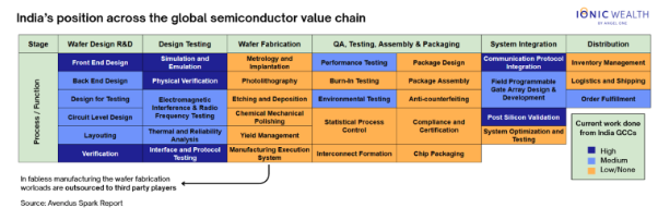
However, wafer fabrication and advanced packaging remain limited, gaps that the policy initiative aims to bridge through upcoming manufacturing and packaging projects across the country
6.2 Indian listed companies in the semiconductor value chain
While India is still in the early stages of building full-scale semiconductor fabrication capacity, several listed companies have already positioned themselves across different parts of the value chain.
CG Power is setting up a ₹7,600 crore chip and power equipment facility, while Keynes Tech is investing ₹3,400 crore in an OSAT unit, both by FY26. Archean Chemicals plans a ₹2,067 crore Silicon Carbide-based chip facility by FY30, and Axiscades Technologies is expanding into chip design and validation.
On the materials side, Acutaas Chemicals, Jubilant Ingrevia, and Stallion India are investing in semiconductor-grade chemicals and gases, ensuring India builds strength not just in chips, but in the ecosystem around them.
7. Conclusion
India’s semiconductor story is bigger than just cutting down on imports. It is about securing the country’s digital future and creating a long-term growth engine for the economy.
With initiatives like the India Semiconductor Mission, PLI, and DLI schemes, the government is setting the stage for global investments and building capabilities across design, packaging, and eventually fabrication.
Of course, the road will not be easy. Challenges like infrastructure, water, and skilled talent need focused solutions. But if India could move from being a mobile importer to an exporter within a decade, it can surely climb the semiconductor ladder too.
This is a $215 billion opportunity in the making. The chip race is on, and this time, India is not watching from the sidelines. It is getting ready to lead.
Disclaimer
This content is intended for informational purposes only and does not constitute an offer or solicitation for investing in any products distributed by or services made available by Angel One Wealth Limited and Angel One Investment Services Private Limited (collectively referred to as “Ionic Wealth”) or any of their affiliates. It is not intended to be, and should not be construed as, advertising or promotional material. The information provided does not constitute investment advice or a recommendation. You are advised to conduct your own due diligence and consult with your legal, tax, and financial advisors before making any investment decisions.
Angel One Investment Services Private Limited is an AMFI-registered Mutual Fund Distributor (ARN 306165). Note that investments in mutual funds and in the securities market are subject to market risks. Read all the investment-related documents carefully before investing.
Enjoying this article
Share it with the world!
Ionic Wealth Newsletter
Investment insights
made simple
Sign up for our newsletter about wealth, markets, and more.


AMFI Registered Mutual Fund Distributor
Angel One Wealth Limited (AOWL)
CIN AOWL - U66190MH2023PLC411784
Angel One Investment Services Private Limited (AOISPL)
ARN AOISPL - 306165
CIN AOISPL - U66190MH2024PTC426203
SEBI Registered Research Analyst Number- INH000020305
Mutual fund investments are subject to market risks, read all scheme related documents carefully.
Registered Office: 601, 6th Floor, Ackruti Star, Central Road, MIDC, Chakala, Andheri (East), Mumbai - 400 093
Copyright © 2025, Ionic Wealth | All rights reserved